
Prime Minister inaugurates SEMICON India 2026 in New Delhi | Current Affairs | Vision IAS

Upgrade to Premium Today

Start Now
MENU
Home
Quick Links

High-quality MCQs and Mains Answer Writing to sharpen skills and reinforce learning every day.

Watch explainer and thematic concept-building videos under initiatives like Deep Dive, Master Classes, etc., on important UPSC topics.

A short, intensive, and exam-focused programme, insights from the Economic Survey, Union Budget, and UPSC current affairs.

ESC

In Summary

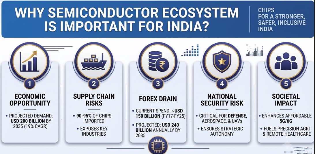
  • SEMICON India 2026, themed ‘Silicon to Systems’, aims to boost India's semiconductor ecosystem and investments.
  • India Semiconductor Mission 2.0 expands outlay to $13.5 billion, focusing on six pillars: design, machines, fabrication, packaging, R&D, and talent.
  • Challenges include limited advanced fabrication, high costs, skilled talent shortage, and slow project approvals.

In Summary

SEMICON India 2026 is jointly organized by India Semiconductor Mission (ISM) under Ministry of Electronics & Information Technology and SEMI (Semiconductor Equipment and Materials International), leading microelectronics industry association. 

  • With theme ‘Silicon to Systems: Building the Ecosystem’, SEMICON 2026 aims to accelerate industry growth and investments, and position India as a key semiconductor hub

India Semiconductor Mission 2.0 (Semicon 2.0)

  • Expanded outlay to $13.5 billion from $8 billion in first phase.
  • Focuses on Six pillars: Design, Machines and Materials, Fabrication units, Advanced packaging, R&D, and Talent development.

Other Initiatives for Semiconductor Industry 

  • ISM (Semicon 1.0) 2021:  To establish a domestic semiconductor and display manufacturing ecosystem. It introduced dedicated Schemes for setting up Semiconductor Fabs and Display Fabs.
  • Research, Development and Innovation Scheme: Supports eligible research projects under Semicon 2.0 and strengthens domestic semiconductor innovation.
  • National Policy on Electronics 2019: Established overarching framework for Electronics System Design and Manufacturing, including core components such as chipsets.

Challenges in India’s Semiconductor Industry

  • Limited Advanced Fabrication: Most Indian fabs focus on mature nodes (>28nm), lagging in advanced chips (3nm, 5nm) for AI and quantum computing.
  • Other issues: High Capital & R&D Costs for Semiconductor fabs; Skilled Talent Shortage in manufacturing workforce; Slow project execution and approval processes etc.

Watch Video News Today

Explore Related Content

Discover more articles, videos, and terms related to this topic

RELATED TERMS

3

Electronics System Design and Manufacturing (ESDM)

An overarching framework established by India's National Policy on Electronics 2019, encompassing the design and manufacturing of electronic products, including essential components like chipsets.

Advanced Packaging

A crucial stage in semiconductor manufacturing where the fabricated chip is encased and connected to external circuits. Advanced packaging techniques are essential for improving performance, power efficiency, and miniaturization of electronic devices.

Mature nodes

Refers to older semiconductor manufacturing process technologies (e.g., greater than 28 nanometers). These are less advanced and typically used for less complex chips compared to leading-edge nodes.

Title is required. Maximum 500 characters.

Search Notes

Filter Notes

Loading your notes...
Searching your notes...
Loading more notes...
You've reached the end of your notes

No notes yet

Create your first note to get started.

No notes found

Try adjusting your search criteria or clear the search.

Saving...
Saved

Please select a subject.

Referenced Articles

linked

No references added yet